Boyuan Technology Co. Ltd
PCIe 3.0 Controller IP
-ultra low resource utilization
-ideal soft PCIe controller for Xilinx FPGAs
Boyuan'sPCI Express 3.0 Controller IP Core,provides high bandwidth、reliable PCIe controller soft solution,which supports muliple lane width (x1/2/4/8) and speed (2.5/5.0/8.0 GT/s)。The PHY interface is in copliance with PIPE3.0,and Equalization interface is in compliance with Xilinx PCIe PHY IP v1.0。
Key Fetures:
- Device Mode:Endpoint(EP)、Root Port(RP)
- Lane Speed:2.5 GT/s, 5.0 GT/s, 8.0 GT/s(support dynamic speed swith)
- Lane Width:x1, x2, x4, x8(not support dynamic width swith)
- Max Payload Size: 128B/256B/512B/1024B
- Interrupt:Legacy、MSI、MSIx
- Optional Capabilities:AER、DSN、LTR、TPH Requester、VSEC
- ASPM:L0s、L1
- PHY I/F:PIPE3.0
- 8 GT/s Equ. I/F:Compliance with Xilinx PCIe PHY IP v1.0
- User I/F:AXI Stream of 128/256bit bus width at 62.5/125/250MHz
- User I/F: full duplex
- Flow Control:configurable total credit and credit for each type
- Data Link Layer: One RAM shared by TX and Replay
- Data Link Layer: Flecible and Fast Retransmit Coponent
- 灵活的重发机制确保数据快速成功重传
- 双时钟设计,链路层LCRC运行在用户时钟域uclk,更易获得时钟收敛
- MAC层去抖动:8b/10b采用寄存器链校准,128b/130b采用同步FIFO校准
- 支持AXI Memory Mapped Bridge:可选
- PHY兼容性:支持Xilinx PCIe PHY,7系列运行在8.0GT/s时需要集成第三方128b/130b软PCS
应用范围
支持数据运算和数据传输应用,尤其适合高性能、低成本、易升级维护和高可靠性要求的应用场景:
- 插入式运算卡
- 芯片直连卡
- 网络接口卡
- 有线/无线通信卡
- 数据通信网络
- 无线通信网络
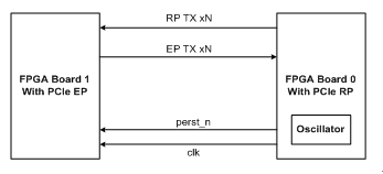
结构示意图

实现示例 A: 3.0x8"
PCIe3.0 RP:
- 最大负载-1024B
- 链路速度-8.0GB/s,链路宽度-x8
- 集成PCIe AXI Memory Mapped Bridge
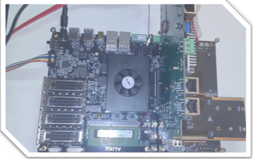
- 实现器件:Alinx Z19-Xilinx xczu19eg-ffvc1760-2-i
PCIe3.0 EP:
- 最大负载-1024B
- 链路速度-8.0GB/s,链路宽度-x8
- 集成PCIe AXI Memory Mapped Bridge
- 实现器件:米联客MZU07A-Xilinx xczu7eg-ffvc1156-2-i
应用层采用Boyuan AXI Master IP:
Resource |
Estimation |
Available |
Utilization % |
|---|---|---|---|
LUT(RP/EP) |
44364/44785 |
522720/230400 |
8.49/19.43 |
LUT RAM(RP/EP) |
960/984 |
161280/101760 |
0.59/0.96 |
FF(RP/EP) |
62806/63706 |
1045440/460800 |
6.00/13.82 |
BRAM(RP/EP) |
43/51 |
984/312 |
4.3/16.3 |
Length |
Memory Write |
Memory Read |
|---|---|---|
BAR-DW |
0.09 us |
1.08 us |
BAR-QW |
0.09 us |
1.08 us |
DMA-1 MB |
6755 MB/s |
6710 MB/s |
DMA-8 MB |
6767 MB/s |
6733 MB/s |
注:测试受到链路稳定性影响。例如链路在数据传输时电源不稳定导致LCRC校验出错,会触发链路Replay,进而对性能造成较大影响。
技术特征
- 针对FPGA应用优化,资源占用率低
- 优化的时序路径,更容易时钟收敛
- AXI Stream数据接口(不带AXI Memory Mapped Bridge)
- AXI4数据接口(带AXI Memory Mapped Bridge)
- 独有的链路层重发算法,消耗RAM资源少
- 独有的链路层CRC运算结构,FPGA设计中易获得时钟收敛
- 流控大小可配置,各类型流控可单独分配
- 可选服务:AXI Memory Mapped Bridge
- 可选服务:AXI Master/DMA Test IP
标准的接口协议
技术支持
从交货日起提供为期6个工作月的免费技术支持,包括电话咨询和电子邮件咨询。技术问题响应时间不超过三个工作日。
功能及时序验证
IP核在发布前,已经通过了大量的仿真,以及必要的FPGA验证。
授权内容
IP核授权方式和技术文件:
- FPGA网表(EDIF)
- 完整的仿真或测试平台
- 综合脚本
- 用户手册,测试报告等技术文档
- 软件驱动,测试例程
- FPGA工程示例
评估/购买:
- : sale@bjbytech.com
- : +86-13601005061